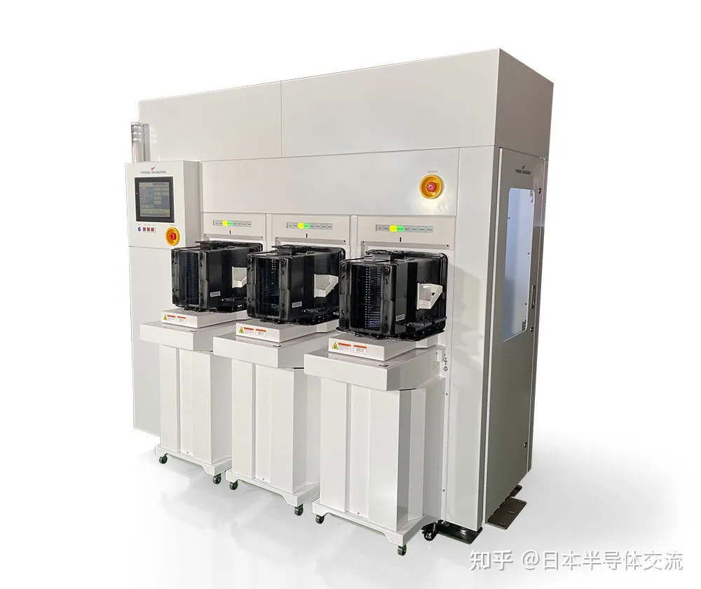
Overview of the Wafer Industry
The global wafer market reached USD 14.7 billion in 2023 and is projected to reach USD 19.2 billion by 2030, representing a compound annual growth rate (CAGR) of 6.3% (2024–2030). By region, the Chinese market has changed rapidly in recent years: from 2016 to 2021, China's semiconductor wafer handling equipment market grew year over year, reaching nearly USD 2 billion in 2021, up 12.05% year on year.
Wafer robots play a vital role in the semiconductor industry. They enable automatic wafer transport and placement, as well as wafer inspection and cleaning, improving production efficiency and product quality. Wafer robots can also perform a range of auxiliary tasks that raise overall line efficiency. As technology advances and wafer processes continue to evolve, wafer robots will find even broader applications, providing strong support for the development of the semiconductor industry.
Wafer Robot Classification
Based on the type of products handled, wafer robots can be classified as follows:
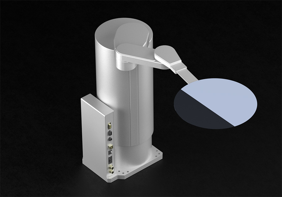
Atmospheric Robot
An atmospheric wafer robot transports wafers in clean atmospheric environments. Its high precision and efficiency make it irreplaceable in semiconductor material handling.
In clean production environments, atmospheric transfer robots complete material handling tasks with precision and efficiency, effectively avoiding the contamination and errors that human handling can introduce. Their unique docking technology ensures stability and safety during transfer, dramatically improving production efficiency and product quality.
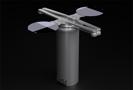
Vacuum Wafer Robot
Vacuum robots operate in vacuum environments, primarily in the semiconductor industry, transferring wafers within vacuum chambers.
Wafer Workstation Components
A wafer workstation consists of an EFEM (Equipment Front End Module), a wafer sorter and wafer carriers.
-
The Equipment Front End Module (EFEM) is an integral part of semiconductor production equipment. Internally, it mainly comprises a chemical vapor filter, air filter, ionizer, wafer transfer robot, wafer aligner, wafer carrier and automated control modules. Among these, the wafer loading system, wafer handling robot and wafer aligner are the three most critical components.
-
A wafer sorter is process equipment used in semiconductor manufacturing. Its internal micro-environment maintains the cleanliness required for wafer transfer operations, enabling wafer off-loading, batch splitting before processing, batch merging after processing, controlled transfer between processes, and final product verification and sorting.
-
A wafer carrier is a container used in semiconductor processing to protect, transport and store wafers — an essential medium for wafers.
iNexBot Wafer Handling Technology
iNexBot offers an advanced wafer handling solution, dedicated to building an efficient and reliable wafer transport and processing system for the wafer market.
Key features of the solution include:
-
Automatic transfer-speed switching: operating speeds can be set individually for each motion command according to wafer inspection, wafer acquisition/output area and other conditions. The host can set these speeds to any value up to each axis's maximum. During operation, the controller automatically changes the transfer speed based on wafer presence detection (via vacuum pressure sensors or wafer presence sensors) or the operation type.
-
Dual-wafer synchronous operation: two wafers can be picked up or placed simultaneously (provided both end effectors are of the same type and positioned identically).
-
Wafer protrusion detection: in some exceptional cases, wafers may protrude from the carrier. Without detection, the wafer and the end effector can interfere with each other, potentially damaging the wafer or the effector. This feature can be enabled or disabled by selecting parameters in the mapping operation command.
-
Wafer mapping: after the robot moves to a specific position in the carrier, it rises from that position and samples the elevation-axis positions where the mapping sensor turns on and off. The sampled data is compared with calibration data to determine wafer status (normally inserted or abnormally inserted), as shown below:

- Interlocking: the system features an interlock function that monitors various states to validate operations, ensuring safe operation.
Robot:
(1) Wafer present: wafer transfer operations are prohibited, such as picking up another wafer / wafer protrusion detection is prohibited / wafer calibration is prohibited.
(2) No wafer: wafer placement and transfer operations are prohibited. Aligner: without a wafer — wafer alignment and calibration operations are prohibited.
In addition, iNexBot's wafer handling technology excels at rapid pick-and-place with transfer throughput of up to 200 wafers per hour. It runs continuously for 24 hours at high speed without power loss or wafer drops, delivering outstanding reliability.

Advantages of the iNexBot Solution
-
Compatible with a wide range of wafer robots — single/double-fork and single/double-arm robots can all use the system.
-
Self-developed system with built-in advanced vision inspection algorithms for high precision and high reliability.
-
Handles wafers of various sizes and specifications to meet diverse transport requirements.
-
High transfer throughput of up to 200 wafers per hour, with strong stability, minimal vibration and no wafer drops.
-
Extremely high precision: iNexBot control systems achieve trajectory accuracy within ±0.02mm, with a trajectory deviation error of ±1.2mm.
-
Built-in safety control interface makes the process controllable, effectively detecting and preventing collisions and accidental injury to improve workplace safety.
Automated Material Handling